Oscilloscope
Jan 2017 - May 2017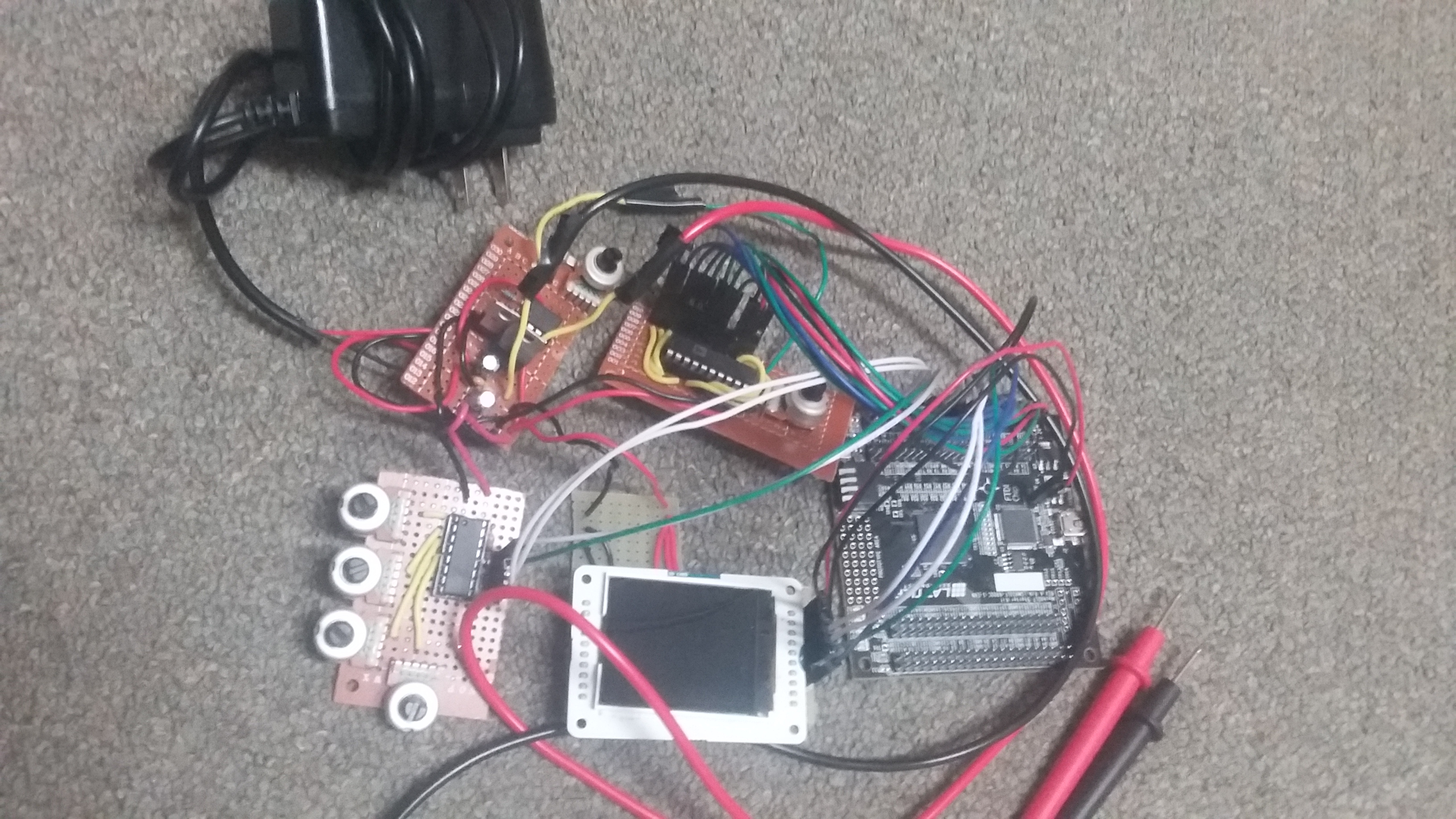
The project is a small 1 million samples per second oscilloscope. The programming was done entirely in VHDL and exists on a Lattice Semiconductor FPGA MachX03 starter kit development board. The VHDL features oscilloscope control logic, a TFT LCD display controller, SPI module, and two different ADC IC interfaces.
The scope control logic samples the ADC every time it updates with new data and calculates the pixel on the screen the data represents given the current magnitude and the time it was received. The screen state is updated with this data and stored in block ram on the FPGA. Once the scope has gathered data for a 10th of a second, it tells the TFT display controller to begin shifting out the new screen state.
When updating the screen, the TFT LCD display controller sends the new screen state pixel by pixel to the display by writing to an SPI module. The SPI module shifts the data out to the screen. The data sent to the screen involves many commands to initiate the screen on startup, to write pixels, and to refresh the screen. These commands were reverse engineered from the Arduino TFT LCD display library, which implement them all in Arduino C code.
In order to accurately begin sampling at the proper time, the oscilloscope logic implements a method of triggering a read every time the input waveform is at the same point in it's period. To determine where in the period a periodic input voltage is, two things are checked:
1. Whether or not the input is at the same magnitude as the last time we triggered
2. Whether the input is rising or lowering
Once a trigger occurs, the input is read until the number of samples read is equal to the number of samples per trigger. This parameter is adjustable by the scopes control knobs. The scope then stops sampling and begins again only once the scope is triggered again. Although this triggering technique doesn't work with all possible input waveforms (for example, functions similar to sin(sin(x)) or other frequency modulated signals) this works with most desired periodic inputs (such as sin(x)).
One fixable issue with this approach is that a falling wave may have some noise which causes it to spike back up above the threshold a small amount while the voltage is decreasing, triggering the reading even though it's falling. To fix this issue, two thresholds are used. These two thresholds, which can be called the "lower" and the "higher" thresholds, must be triggered in succession using the earlier two rules to cause a trigger to happen. This way a falling voltage with a small spike cannot cause a trigger as it was not previously below the lower threshold when the spike occurred. This low and high threshold are displayed on the LCD display when the user changes the input control knobs corresponding to the threshold.
To read the controls, the FPGA communicates with a second ADC using another SPI controller which reads four potentiometers. There is one potentiometer to control the center threshold, one to control the distance the high and low thresholds are from the center, and two to control the length of the sampling after the scope is triggered (one for course adjustments and one for fine).
The input to the oscilloscope has a buffer stage with variable gain using a single high input impedance, high frequency op-amp. The input gain is varied using a potentiometer connected to the op-amp to form a basic non-inverting amplifier circuit which is used to adjust the input gain. There are two scope leads soldered to the board, one of which is connected to analog ground and one of which is connected to the op-amp's non-inverting input.
The power comes from a 12V DC wall socket, which powers a 6V regulator and a 3.3V regulator. There are multiple supply voltages inherited from this one supply which may be confusing if not explicitly stated how they float relative to each other:
| Name | Voltage relative to negative terminal of DC input: |
|---|---|
| | |
| | |
| | |
| | |
| | |
| | |
| | |
| | |
Note that the "Analog" ground floats 6V above the "Digital" ground and thus analog input values are just their voltages relative to the negative terminal of the DC input offset by 6V.
The two scope leads are connected one to the input op-amp buffer and one to the analog ground. The op-amp input is powered by the analog -6V and analog 6V supply, allowing an approximately 9V range in the input (between analog -4.5V and analog 4.5V) as the op-amp only works to within about 1.5V of either rail. The signal from the op-amp is then divided relative to the digital ground down to a range useable by the high speed ADC.
A 3.3V supply is used to supply power to the FPGA, both ADCs, and LCD display. It is also used in an over voltage protection circuit to protect the main ADC from possible over voltages which may result from misuse conditions such as applying greater than 12V between the two input leads.
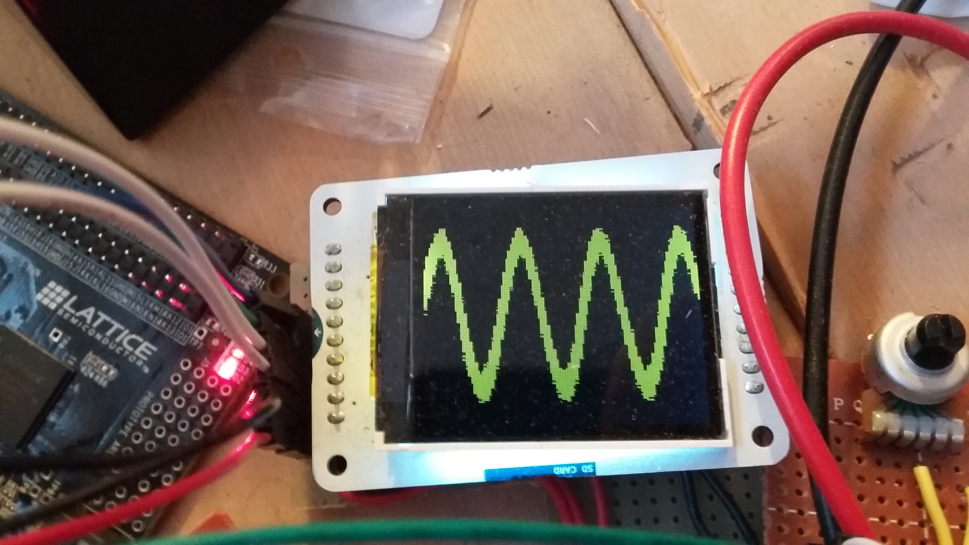
This picture and video show the oscilloscope reading an ~50KHZ sine wave generated from a Colpitts oscillator. In the video you can see the wave being read in yellow and the low and high thresholds represented by a blue block. Note that when the two thresholds are placed too close together in the video, two waves 180 degrees out of phase are shown instead of a single wave. This is caused by the issues outlined in the Triggering section.
There are many improvements that could be made on this build. Specifically increasing the max frequency, displaying more information, and using a more digital approach would be the most important improvements.
The maximum frequency can be increased by buying a faster ADC and clocking the FPGA from an embedded PLL rather than an on board oscillator. A faster ADC wasn't selected in the first place mainly to keep all the soldering through-hole.
Displaying more information would involve writing code to display the magnitude of the voltage being read and the time passing. To display more complex data like numbers on the screen using just VHDL starts becoming tedious, and so it would be quite useful to rewrite a large amount of the code, using the FPGA for digital signal processing only and using a separate micro-controller for the display. This would also allow a much higher level of manipulation of the data, and so many other useful ways of dealing with the input data could be included such as averaging the waveform for a smoother display, allowing automatic magnitude calculations, or many other similar operations many consumer scopes have.
In order to display values for the magnitude of the waveform it would make sense to use a higher resolution ADC and zooming into the signal digitally rather than using analog amplification. This is because it becomes quite difficult to determine the actual magnitude of the original signal accurately after it's been amplified. A higher resolution ADC approach would mean amplifying the signal digitally using the FPGA. This would allow the FPGA to now know the original amplitude of the signal before the amplification, and so the real magnitude is easy to display accurately.