RadIO V1
(Jan 2019 - May 2019)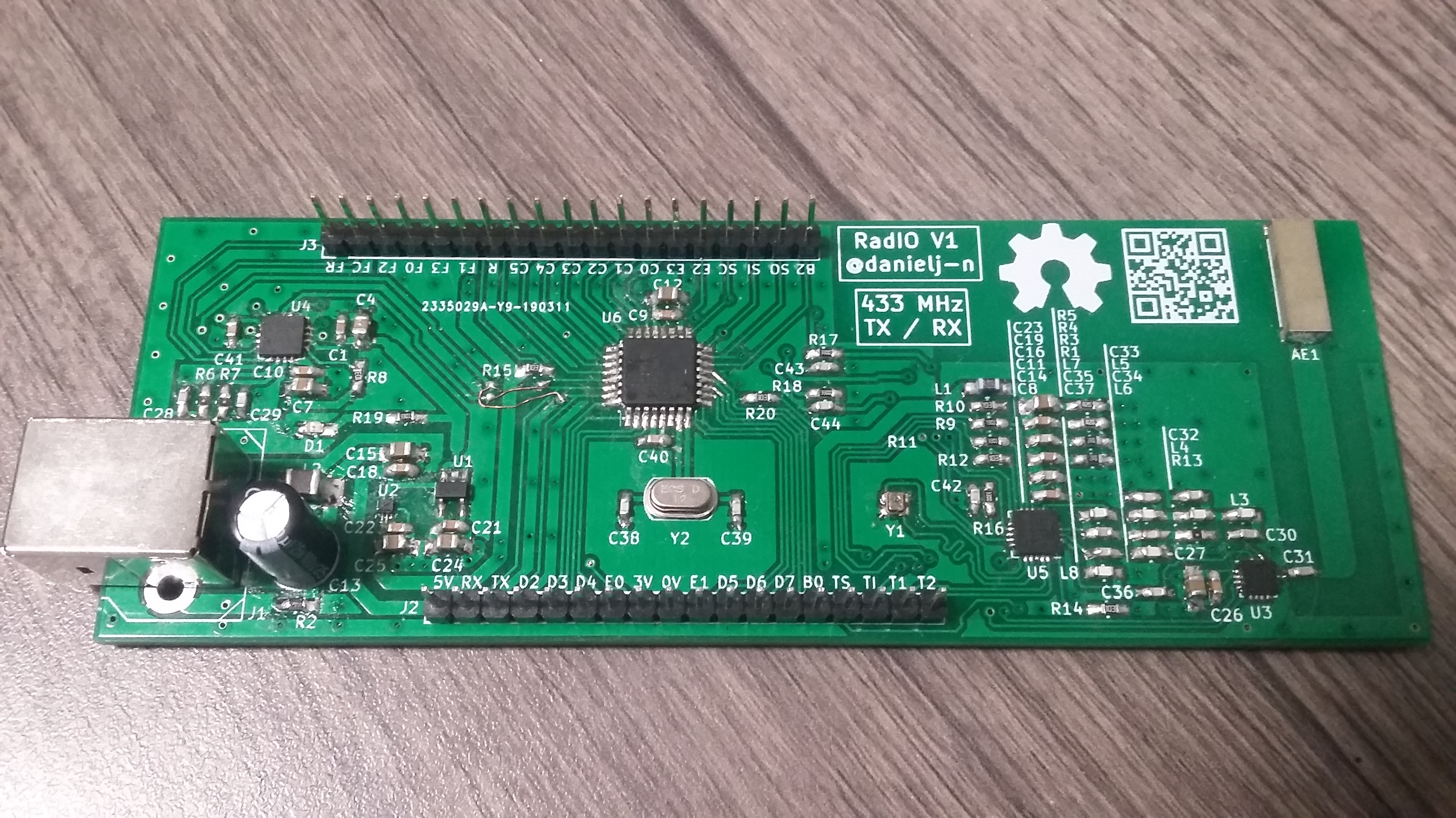
RadIO is a microcontroller board with integrated digital radio communication, based around the atmega328pb microcontroller and the Si4464 transceiver. The board is powered over a USB cable and features a uart to USB IC which can communicate with a computer connected over USB. GPIO unused by the microcontroller to control the radio and usb ICs are broken out. While the Si4464 has the ability to communicate on a range of frequencies from around 200 MHz to 900 MHz, the hardware is build to operate on channels around 433 MHz. The maximum baud rate and bandwidth of the device is currently untested but should be around 500 kbps and about +-5 MHz around 433 MHz (although behaviour may be significantly degraded near the edges). The maximum output power of the Si4464 is around 20 dBm, but the exact output power one may get depends on the design and has not yet been experimentally determined for this build. The PCB design was done in KiCad.
The hardware surrounding the Si4464 is mostly calculated using the methods outlined in two Silicon Labs application notes on the design of the hardware for the Si4464. This hardware features a transmission filter and matching network, power filter, receive matching network, rx/tx switch, and antenna and feedline.
Since the switching power amplifier of the Si4464 generates a squarewave output (and likely contains other sources of distortion) the transmission output of the IC must be filtered. This is done using a high order Chebyshev filter to attenuate all frequencies higher than approximately 433 MHz. There is also a notch filter which allows the higher frequency harmonics to see an impedance of roughly 50 ohms while still being attenuated by the bandpass to prevent harmonic reflections, which may or may not be required. As a filter of this high a frequency tends to require very small component values, parasitics tend to change the value significantly from what would be optimal.
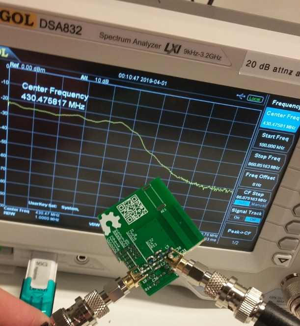
While simulation of these parasitics is one option to better optimize the system which may or may not work, an alternative option of simply building the filter, testing it, and fixing it was used instead. The filter section was removed from the PCB, and had calculated values of inductors and capacitors soldered onto it. SMA connectors were soldered onto the input and output of the filter network to attach the device to a high frequency function generator and spectrum analyzer. This device can be set up to act similarly to a vector network analyzer, only without a phase plot and only a received power plot. This is enough to optimize the filter in this particular case.
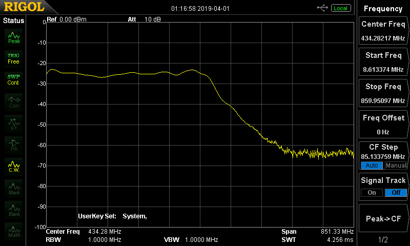
Starting with values near the calculated, the bandpass with parallel notch filter was tested. The frequency where attenuation occured was found to be far off from optimal as predicted, a couple other values were guessed and at tried. Eventually a fairly optimal configuration was found using the values of passives available.
This filter section was built without a proper transmission line. This was because a double sided design was used with a standard board thickness of 1.6mm, which means that a 50 ohm transmission line must be very wide (120 mil). The total length of the section was short enough that a 433 MHz signal would likely not see significant transmission line effects (the line is around a 10th of a wavelength long or so) and so this was simply accepted. Due to this, the usefulness of the notch filter to keep a 50 ohm load present at higher frequencies is debatable, but still included for completeness.
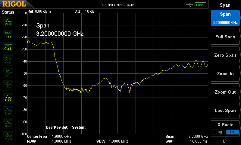
This lack of transmission line is thought to also be the reason for the bandpass filter's bad response into the GHz, although the exact reason for this remains unclear. This effect may still not be horrendous as the bandpass filter still provides some attenuation, the chip antenna's bandpass response itself should attenuate out of band signals (although the traces themselves may radiate), and the square wave signal contains less content at these higher frequencies, however it is far from truly optimal. The significance of this issue can be determined using an SDR once transmission has been achieved using the board.
Below is the setup with the filter cut off the board with some passive components and SMA connectors soldered on to it, connected to a spectrum analyzer to characterize the filter.
Below is the resulting spectrum readings after some fiddling around with components. At lower frequencies attenuation is fine, however at much higher frequencies attenuation starts decreasing significantly.
The power filtering for the Si4464 is an LRC circuit, the LC being the filtering portion and the extra Rs being used to help prevent resonance and specific frequencies. To determine these resistor values, a spice simulation was performed starting with a simple LC circuit with the standard high frequency power filter capacitor values of 100pF, 1nF, 100nF, and 10uF, and a 100nH inductor to supply decent attenuation at ultra high frequencies with a high enough self resonant frequency to not be an issue. Series inductors and resistors were added to each of the capacutors to simulate more realistic behaviour. The simulation of course found a number of resonant points in this circuit without any additional added in resistors and so various extra resistors were added in series with the capacitors. When these resistors significantly negatively effected the filtering abilities of the circuit, a new capacitor was added in parallel with the resistor placed in series and the older capacitor ignored, so that the filtering would still be applied however the frequency response was less effected. The end result of this was the power filter network.
Although this network is similar to the transmission filtering in that it may behave better or worse depending on circuit parasitics, it is likely less sensitive and less important to optimize. Thus, this circuit was left unoptimized past simulation.
The receiver matching network is unchanged from simple calculations using the methodology presented in the application notes, and rounding to easily findable values. While the passive values here are very small much like the transmission network, the matching abilities were more difficult to double check using the same method due to the Si4464's internal receive circuit itself being significant in the matching. If the matching is off this will likely only result in a decrease in power received rather than an out of band transmission, and there are less components than the transmission network making the circuit is likely less sensitive to some values being off.
The receive network also does not have proper transmission lines for the same reasons as covered in the transmission network discussion. This is likely less of an issue than the transmission network as the 433 MHz frequency that is trying to be received will not likely see significant transmission line effects due to line being short.
The rx/tx switch is used to switch between transmitting and receiving on the board. The switch is integrated nearly identically to the method in the data sheet, and controlled by the Si4464.
While the board is not significantly space constrained and so a PCB antenna could have been implemented, in order to keep the design simpler a chip antenna was used instead. An SMA jack to a swappable antenna could have also been used, and may be used if a second version of the board is made. The chip antenna chosen has a bandwidth of about 10 MHz, and is probably the main constraint on the bandwidth of the whole board.
The antenna being far away from the rest of the circuitry requires a long transmission line leading to it, calculated using an online calculator. As a fairly thick two sided board was used, this transmission line has to be quite wide to match with the antenna's 50 ohms, around 120 mil wide. Via fencing around the tranmission line helps prevents radiation from leaking.
Other than the radio related hardware, other hardware is integrated onto the board to control the radio and add useful peripherals. These are the microntroller, UART to USB, and regulators.
The atmega328pb was used as it was the cheapest Atmel microcontroller with enough extra GPIO to likely satisfy most applications, a clock speed higher than 10 MHz, and the ability to be clocked using just an external crystal and capacitors. Atmel microcontrollers were desired simply due to having used them in the past making programming easier.
The FT2302 was used as it allowed for very simple interfacing between the microcontroller and USB over UART, and is made by the well known chipmanufacturer FTDI. Note as well that using an atmega328 and FTDI chip makes this board an Arduino Uno clone, a reasurring mark that this is the right track.
Two voltage regulators were used, one for the 3.3V to power the transceiver and microcontroller, and one 2.8V to power the antenna switch. The UART to USB chip is powered from the filtered 5V from the USB input.
While there are many aspects of board layout to consider in any design such as limiting current loops, grid aligning components, etc. Two notable aspects of this design are the via stitching and local ground planes.
Vias were placed around the board spaced out by approximately a 1/50th of at wavelength of 433 MHz, and somewhat larger where this wasn't possible. This is used to prevent radiation from the RF section of the board from bouncing into other sections of the board, and is generally done at around 1/20th or 1/30th of a wavelength, however 1/100th was chosen as it was easily doable, and more should be better than less.
Local ground planes are used to prevent two seperate parts of the circuit from interfering with eachother. Generally this is done with digital and analog ground planes, however there is some debate as to it's usefulness in other applications. Although seperate ground planes, when done properly, should end up with a better design featuring less interference between sections, it often leads to significantly increased inductance on traces entering and leaving the local ground plane, and isn't seen very often outside of seperating digital and analog grounds. While I attempted this technique experimentally on this board, there are a number of places where it didn't end up working as well as desired, and likely isn't required to this degree. For this reason this technique will probably be avoided unless otherwise advised in the future. It's difficult to say whether this will have a positive or negative effect on this particular board.
Programming was done entirely in C, using gcc-avr as a compiler and avrdude to program the flash on the microcontroller.
The microcontroller communicates with the Si4464 over an SPI bus, where it can send commands to boot up and configure the device. While much of this is documented clearly in the downloadable API documentation which Silicon Labs supplies, some of the configuration must be done using a Silicon Labs Windows GUI downloadable from their website. This program spits out basically all the commands needed in order to configure the device.
To properly run this on Linux, one must run wine, as well as install the newest version of the .NET framework that currently works with wine (around version 3.5 if I recall correctly). After booting up the GUI, one can select the specifications they desire and out pops a dump of a number of command names and values to pass. To properly convert this command sequence to the format desired by the C code, a small python program was written.
Most of the code written is within a library specifically for the RadIO which allows setup of all of it's various peripherals and control over the radio and other peripherals using library function calls and objects. The library imports the 3rd party avr io.h library which allows easy to remember register names to be used for easier code writing. The code is currently as simple as possible while still allowing configuration of a simple network of RadIO boards. The code is written in such a way that alternate network types and configurations should be easily addable in the future if desired.
While this initial version of the RadIO will probably work, a lot of improvements can be made. Some improvements are highly desired to make the board work better, while some simply increase functionality in different ways. These include adding a bootloader, fixing the ismall hardware issues, upgrading the board to four layers, giving the board a higher power output, and increasing the board's spectrum coverage.
In order for easier reprogramming of the board without a 3rd party programmer, a bootloader can be written which allows the board to be self programming. This will likely be done in assembly as the code must be small, and allows for easier direct control over memory.
There are a number of fixes or changes that were mentioned earlier, as well as others that could be added to improve the board. These include replacing the chip antenna with an SMA jack, possibly getting rid of the local grounds, fixing the transmission lines on the recieve and transmit, and fixing the overall RF layout quality. A lot of these modifications can be done more easily by switching from a 2 layer board to 4 layers, so that will likely be done as well. The TX and RX UART lines are also backwards and had to be switched using extra wires soldered onto the board, which must be fixed in a layout update.
Higher transmission power is desireable, as this allows communication over a longer distance. While the power of the Si4464 by itself should allow for communication indoors of similar range to that of WiFi or BLE, a much higher power signal may be able to reach distances similar to that of walkie talkies and still be within legal broadcast limits. This extra power would have to be gained using an amplifier of some sort, possibly built from discrete parts as there are few ICs in the desired frequency range with the desired power output (around 5W).
Larger spectrum coverage would be nice to allow for a broadcasting or receiving on very different frequencies if one band was too busy, as well as receiving and decoding signals from other devices that would be handy to hack such as blue tooth receivers or similar devices.