Synth
(Sept 2017 - Oct 2018)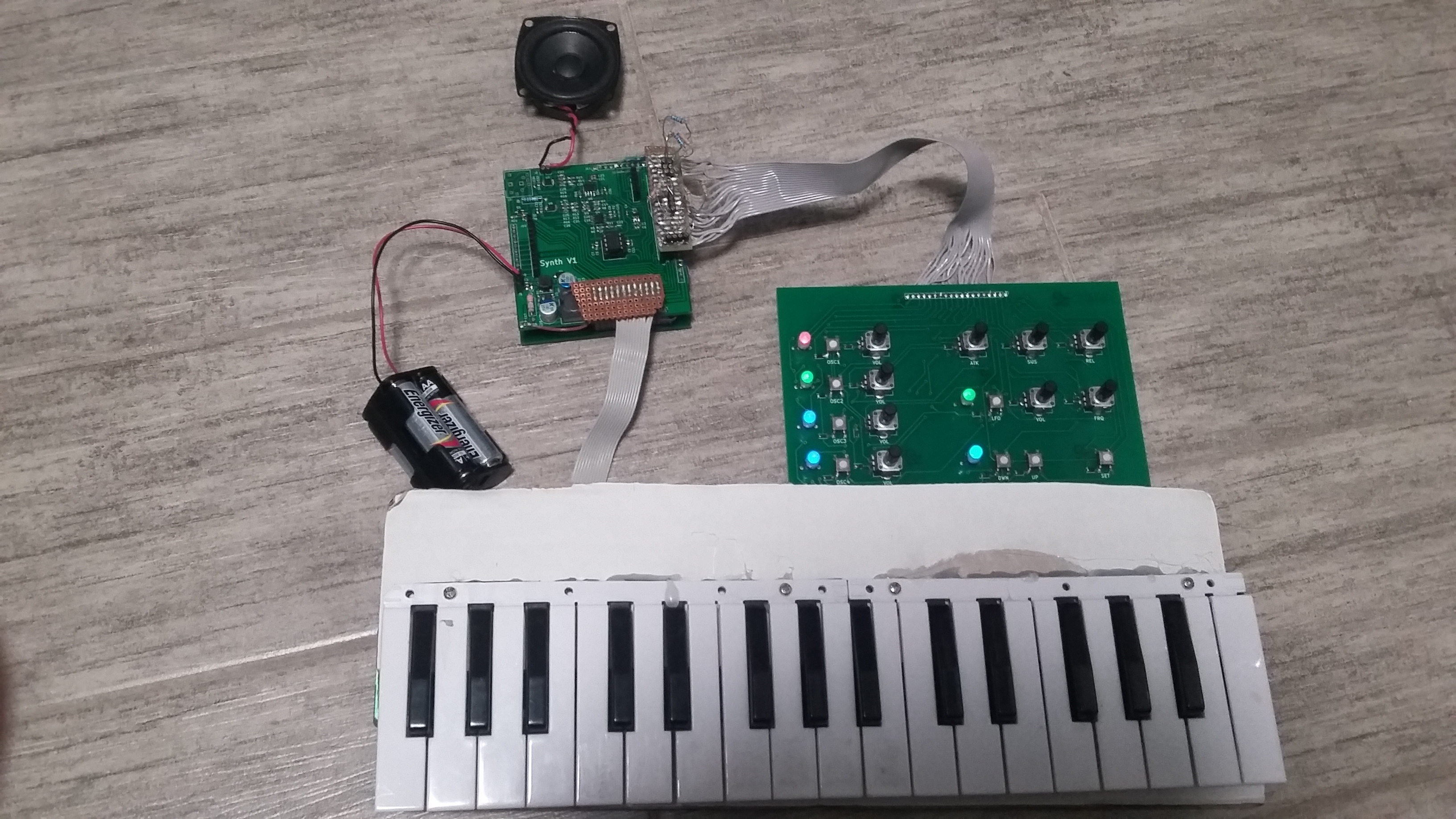
The synth is a 32-bit ARM micro-controller based synthesizer, based on the operator synthesizer bundled with the digital audio workspace software Ableton Live. Note that this digital synth is simply the basis for the project: No code was taken or based off of this digital synthesizer, rather the higher level workings of the project like number of oscillators, what type of wave shapes, and what types of envelopes are based off of this synth. The firmware is written entirely in ARM-C.
The synth has a 32-key keyboard (taken from a toy keyboard), a control PCB board with potentiometers and buttons to control the sound, an MCU board with the microcontroller, and a main board which has all of the power and audio circuitry on it. The synth has eight voices, four oscillators with configurable frequency offset, one LFO, and a three part envelope, all digitally synthesized with the micro-controller. All part numbers for ICs and component values can be found on the schematic for this project.
The firmware features three main parts: the setup, the interrupt, and the main loop.
The setup essentially sets up all the special purpose registers to their proper states. This is done entirely by directly writing values to addresses. This setup turns off the watchdog timer (which is for some reason default on), activates fast flash for high speeds, configures the external crystal to be used and multiplied up to the desired frequency with internal PLLs (120 MHz), configures the ADC, sets up all the basic GPIO, sets up SPI, and finally enables interrupts.
The main loop is used for polling all of the user input hardware. It continually reads all of the ADC values, checks if any new buttons have been pressed, and checks if any new notes have been pressed. If any of these ADC readings or button values change, certain variables or arrays are updated to be used by the interrupt. For example, every time a key is pressed on the keyboard the key is added to a fixed length queue of up to eight keys, which is later read by the interrupt. Although all the potentiometers are linear, some of the potentiometers have their values transformed in order to emulate non-linear potentiometers such as log pots.
The interrupt is used to update the state of the DAC at regularly spaced intervals. When the interrupt is triggered, it begins a process of looking at what keys are being pressed, how long they've been pressed for, what oscillators are on, what detunes are set on each oscillator, and other factors to calculate the exact amplitude to be written out next to the DAC. The interrupt runs at a maximum rate of 40 KHz, which is configurable in the code.
One aspect of this process that others have been curious about is how different frequencies are generated. For example, let us say that there is just one note being held down with one sine wave oscillator running. The sine wave is generated by looking at a look up table of 2000 values which represent amplitudes of a 20 Hz sine wave, sampled at 40 KHz (the maximum rate at which the DAC is updated). So if each of these values were written to the DAC one by one, updating the DAC at 40 KHz, a 20 Hz sine wave would be produced. If the note we actually want is, say 100 Hz, the program simply begins skipping values. At 100 Hz, in order to get through the whole array of to the DAC in a fifth the time, the program must look at every 5th value rather than every value. Using this technique, frequencies can be generated from 20 Hz to frequencies near the nyquist frequency, one half of the DAC update rate (maximum 20 KHz). Of course, frequencies, near the nyquist become distorted as the number of samples decreases. However, as human hearing is limited to around 20 KHz, this distortion is not audible until one is near the edge of human hearing. These are mainly frequencies which are too high to be exceedingly pleasing and so are not often used musically.
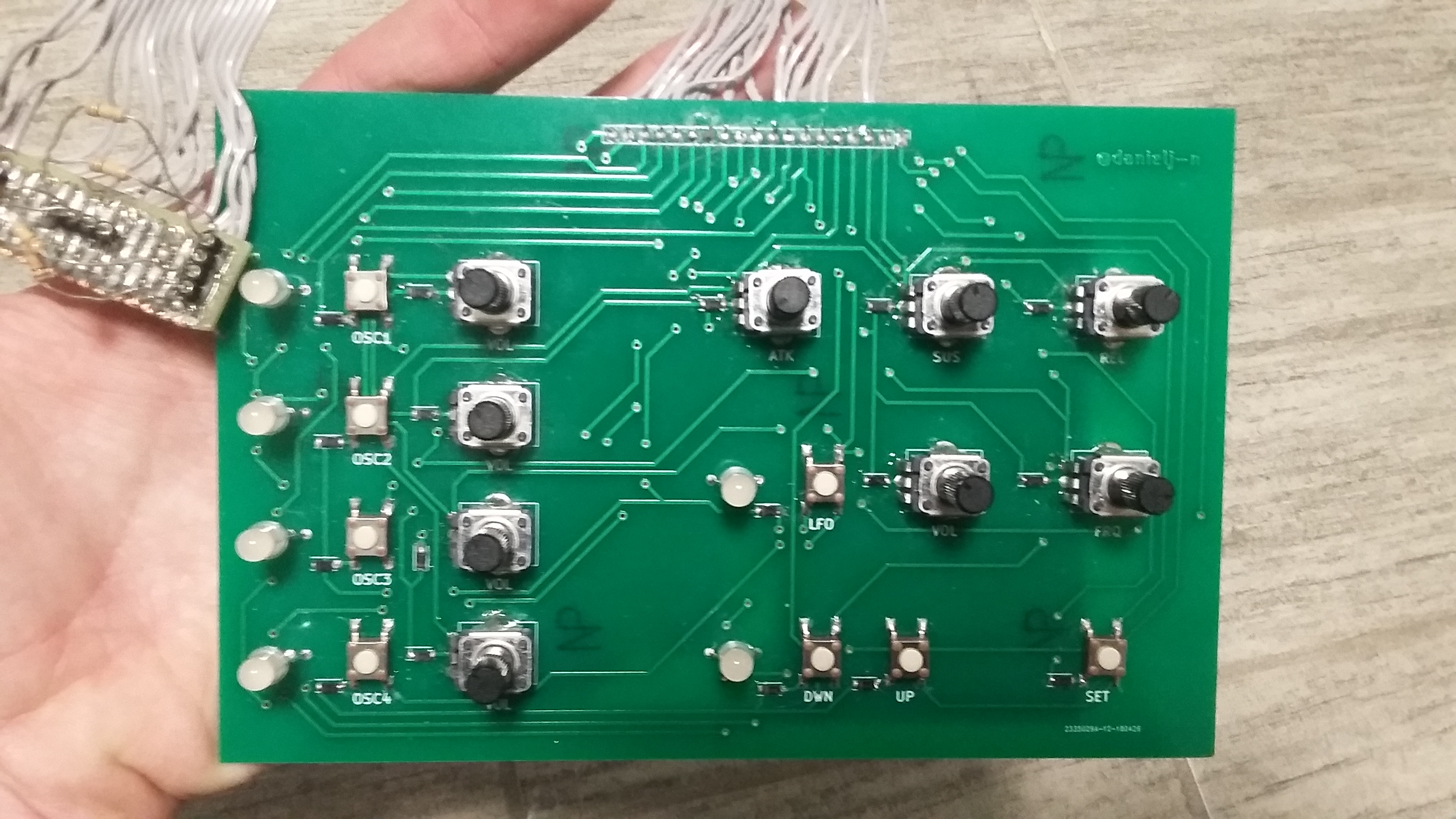
The control board was the first circuit board created. The board can be broken up into four pieces: Main oscillator control, LFO control, envelope control, and offset control. Each of these pieces feature buttons, potentiometers, and RGB LEDs which are controlled using a matrix setup in order to limit the number of GPIOs that have to be used by the microcontroller.
The four main oscillators each have a button, a potentiometer, and an RGB LED. The button switches what wave shape the oscillator should be every press, selecting from four different oscillator types: sine, triangle, square, and sawtooth. The RGB LED changes colour to reflect this change. The potentiometer is used to control the volume of the oscillator.
The LFO oscillator is controlled nearly identically to the main oscillators with a button, RGB LED, and potentiometer, however it also features one extra potentiometer. This extra potentiometer controls the LFO frequency, over a range which is configurable in code. This range is currently approximately 1/5th Hz to about 20 Hz.
The envelope control is made of three potentiometers which control the attack (time it takes for the note to reach maximum amplitude), sustain (time the note lasts for if the key is held down) and release (time the note takes to dither back to zero after the sustain is finished, or the key is released).
The offset control is used to control the frequency offsets to essentially map notes on the keyboard to different frequencies. Two buttons go up and down octaves, and the octave the user has currently selected is displayed with another RGB LED. There is one final button which is used for detuning individual oscillators. When this button is pressed, the user selects an oscillator (by pressing one of the main oscillator buttons) and an offset (by pressing one of the keys on the keyboard). This offsets that oscillator's frequency by a certain amount based on the key that was pressed.
There are also a number of extra external resistors placed on headers on the control board's cable which goes to the main board. Four of these resistors were added due to the MCU not allowing pull down resistors on ADC pins, and three of these were added to allow for the brightness of each of the colours in the RGB LEDs to be tunable. More about these in "Further Improvements".
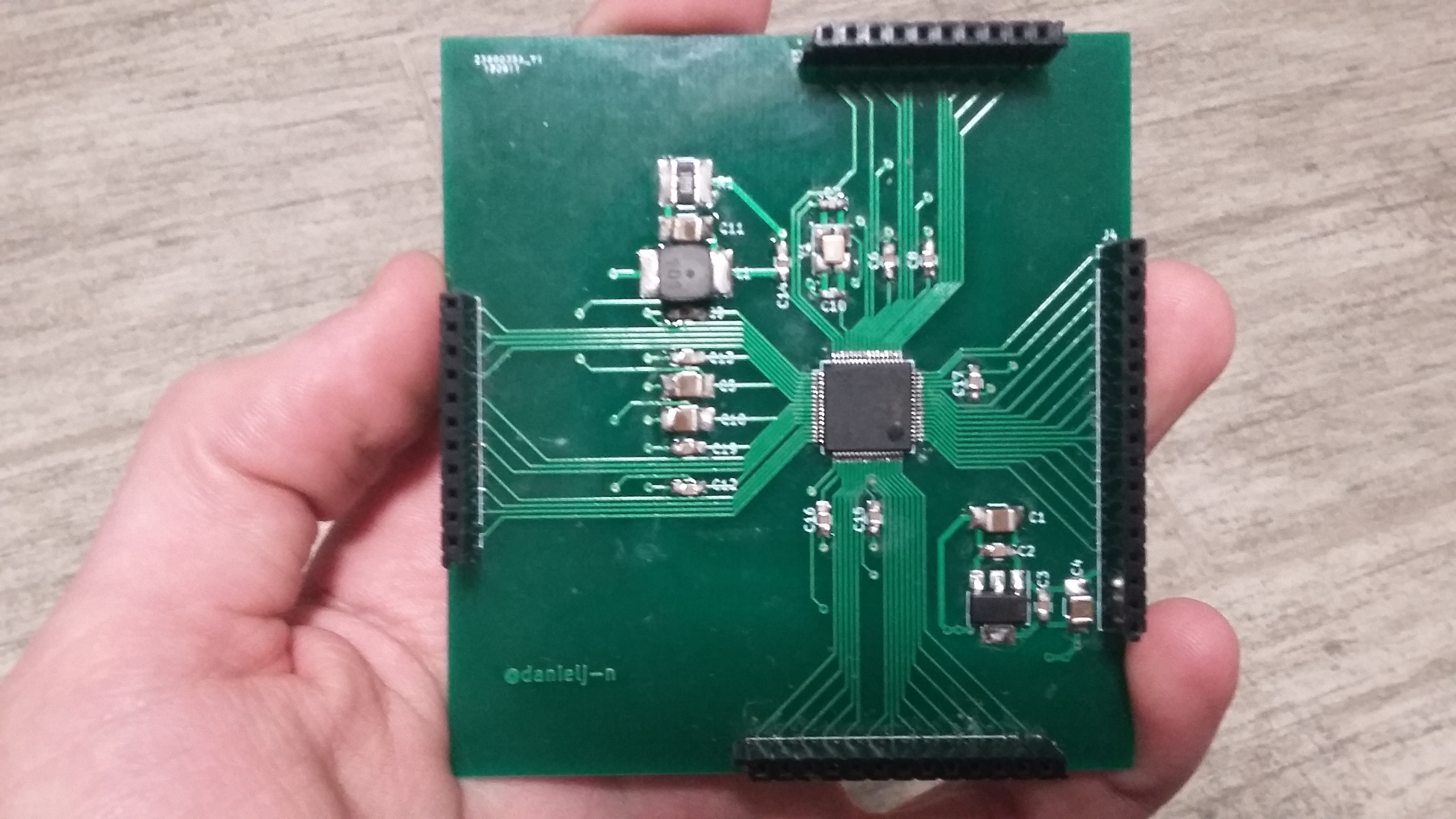
The MCU Board contains the 32-bit ARM microcontroller, breakout pins for connecting to every GPIO, a voltage regulator to bring down the input voltage to 3.3V for use with the MCU, and recommended bypass capacitors and power filtering.
The board is based off of the Atmel SAM4S Schematic Checklist PDF which I attempted to replicate as closely as possible. A link to this PDF can be found on the schematic for this board. The PDF mostly tells the designer to place bypass capacitors but also recommends heavier LCR filtering to be placed before the PLL power input as the PLL power input requires better regulation than the rest of the board. This LCR circuit was designed with the help of a custom Matlab script used to estimate values for the resistor in the LCR filter which is used simply to kill oscillations that result from an LC filter.
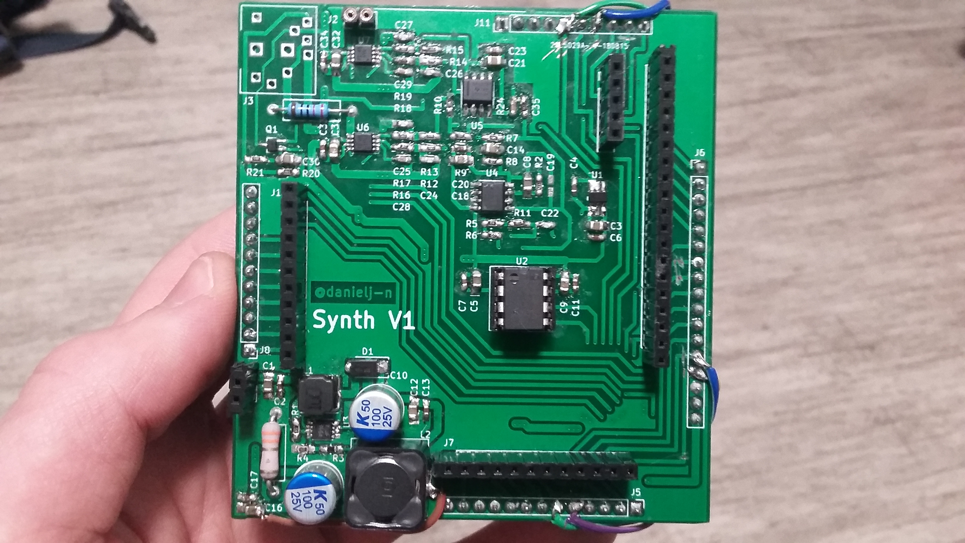
The main board is the most complex circuit board in the device and contains most of the hardware the project needs to function. The main board can be broken up in to five main sections: Power, DAC, preamp, power amp, and headers.
The whole project is powered with three AA batteries which have a range from about 4.5V to 3V in series before they begin quickly dropping in output voltage. The board requires 5 volts for the DAC and audio ICs to function and so this 4.5 to 3 volts is stepped up with a boost converter. As the boost converter may be quite noisy, a 2nd order filter is used to reduce noise significantly. The switching regulator used is of a gated oscillator configuration and so the filter should be placed outside of the feedback. There is an error in the schematic and board which shows the filter in the feedback network, however this is fixed using cut traces and soldered on jumpers (more details on this and other fixes in the "Further Improvements" section). This whole power section of the board is kept somewhat isolated from the rest of the circuitry by placing it as far away from other components as possible, and extending the bottom ground plane to the top of the board for a small section for superior shielding.
The DAC is a 16-bit DAC, which splits it output into linear divisions of a 2.5 V external voltage reference. This external voltage reference as well as the DAC output are both buffered as they both have fairly high output impedances, as well as filtered to remove significant noise.
The preamp stage is fed directly by the DAC and acts both as the DAC buffer, as well as an interface between the DAC voltage levels and the amplifier voltage levels. The DAC outputs a single ended 0 to 2.5 volts, however both the op-amps used for buffering as well as the audio amplifiers require a voltage further from the rails than this. Exact data sheet specifications were used in design, however for simplicity of explanation for now it can be assumed this was about 1V above ground and 1V below power (5V). To achieve this, op-amps were used to offset the signal by 1.25 volts to a range of about 1.25 to 3.75 volts. In order to interface with the audio amplifiers it's also required to generate a differential signal from the single ended DAC output as the audio amplifiers require a differential signal to function, as well as simply for the sake of noise immunity. This is done with further op-amp circuitry, to generate an inverted 1.25 to 3.75 volt signal to be used as the negative of the original.
The power amplifier stage has some final filtering on the inputs of the ICs to remove any noise, before outputting the power to the speaker and headphones. There is a separate amplifier for both the headphones and the speaker as the added complexity in switching the high fidelity signal with minimal distortion wanted to be avoided. The amplifier ICs and support circuitry were approximately the same price as any optimal audio switching solutions such as mechanical relays anyways, so this was decided to be the optimal solution.
Finally, there are all of the headers on the main board. There is a header for an extra board which could be added if desired which connects to all remaining unused GPIO on the microcontroller, as well as another header used to program the MCU using a 3rd party FTDI based programmer board. Headers to attach the keyboard and control board are used rather than directly soldering these separate boards onto the main board in order to keep the project somewhat modular which is easier to carry around. All remaining headers plug directly into the microcontroller board to interface with GPIO and apply power to the microcontroller, acting like a shield (as in "Arduino shield" not "noise shield") for the MCU board.
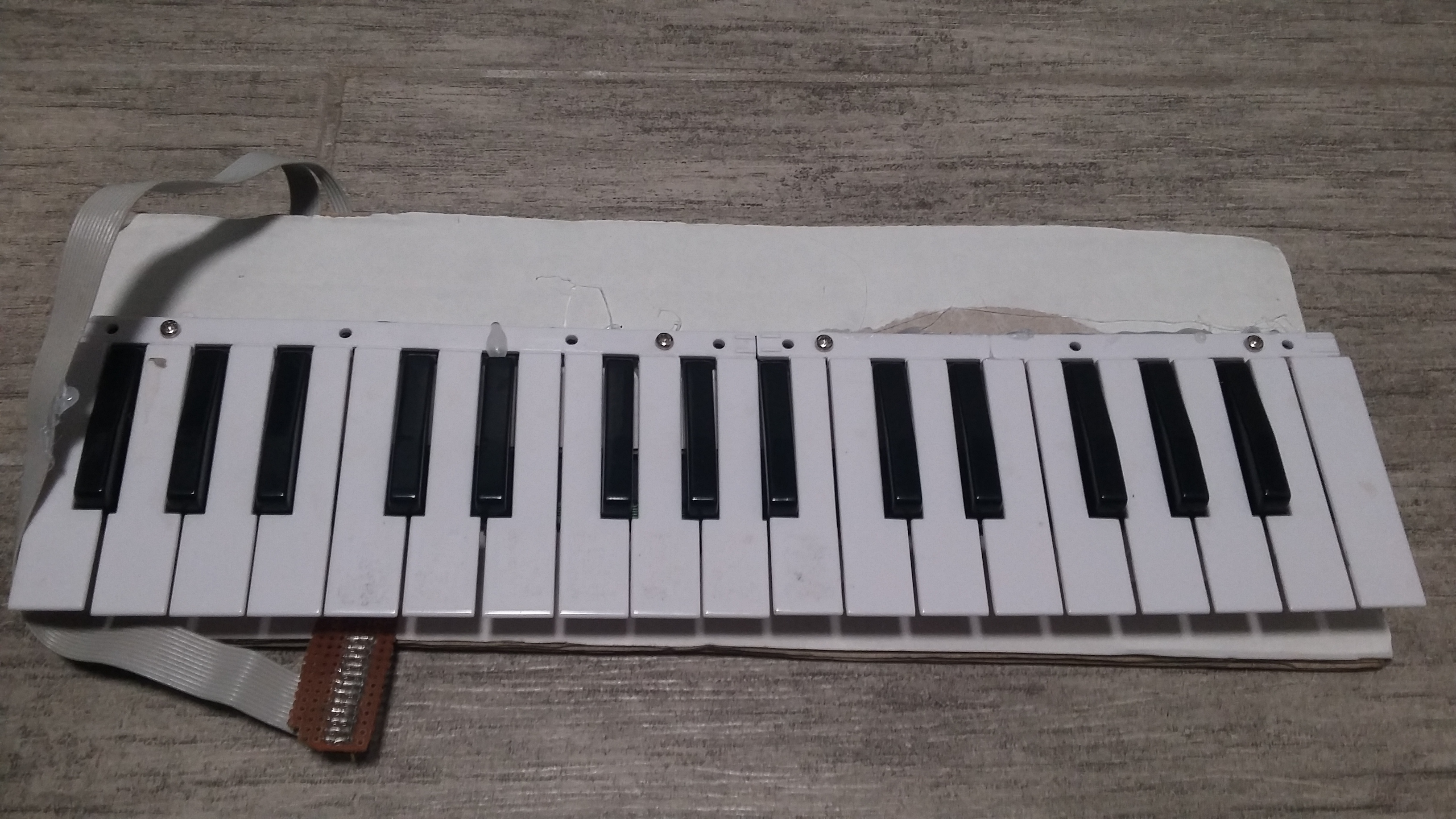
As the keyboard was taken from a child's toy I had in my attic, it's workings had to be reverse engineered. It turns out the device was a simple button matrix, with each key acting as a button. This button matrix is sampled by the GPIO on the microcontroller in a similar fashion to the control board.
In order to put the keyboard back together after ripping it out of the toy, some cardboard was glued to the circuit board and keys in order to hold everything together better.
On the main board I added a solder mask which specified "Synth V1". This was because I knew there would likely be errors with the circuit as the whole project had never been breadboarded before populating the main board PCB. A Synth V2 main board may be made in order to fix these issues, most of which are currently fixed using soldered jumpers.
These issues are mainly simply mis-connected GPIO or errors in the silkscreen and so are easy to fix however there are a couple issues like the aforementioned problem of the power filter being in feedback loop of the regulator or extra resistors that need toe be added to the control board. These issues take some analysis to fix however aren't much of a problem overall and should be taken care of for the 2nd version of the synth.
Two main hardware additions that would be very useful to add would be an on off switch, and an LDO after the switching regulator to reduce potential switching noise. No audible noise has been noticed coming from the speaker, nor has any significant noise been noticed by an oscilloscope (with a not super accurate range of around +-10mV), however it is likely a good idea regardless.